이 글은 TI 사의 slla120.pdf /Interfacing Between LVPECL, VML, CML, and LVDS Levels 문서를 보고 고속신호 규격 부분에 대해 정리한 내용이다.
참고자료는
TI사가 발행한 문서
scaa059c.pdf/AC-Coupling Between Differential LVPECL, LVDS, HSTL, and CML
scaa062.pdf/DC-Coupling Between Differential LVPECL, LVDS, HSTL, and CM
slla120.pdf Interfacing Between LVPECL, VML, CML, and LVDS Levels
다음 3가지 문서가 high speed signal standard(LVPECL, CML, VML, LVDS)에 대한 설명을 다루고 있다. 또한 규격이 다른 standard를 어떻게 연결해야 하는지에 대해서도 다룬다. 예를 들어 LVPECL ouput을 LVDS input에 연결하려면 termination이나 전압을 어떻게 biasing 해야 하는지에 대해 적혀있다. 고속 신호 규격의 종류도 많고 termination 방법도 많고 biasing 방법도 많아서 전부 정리하긴 어렵다고 느꼈다.
그래서 다음 문서를 보면서 내가 알게 된 부분과 용어에 대해서 중점적으로 작성하였다.
1. LVDS, CML, VML, LVPECL의 common mode voltage와 swing voltage, 그리고 회로 내부구조
2. AC coupling, DC coupling
3. termination과 biasing
4. 예시
1. LVDS, CML, VML, LVPECL의 common mode voltage와 swing voltage, 그리고 회로 내부구조
differential line으로 고속 통신을 하는 신호규격에는 정말 여러 가지가 있다. 칩 데이터 시트를 읽을 때 주로 볼 수 있는 신호규격으로 lvds vml cml lvpecl이다.
lvds - low voltage differential signaling
vml - voltage mode level
cml - current mode level
lvpecl - low voltage positive/pseudo emitter coupled logic
처음 봤을 때 저 단어들이 하나도 안 들어온다. 왜 저런 단어들로 명칭을 지었는지는 slla120.pdf 문서를 보면서 어렴풋하게나마 알게 되었다.
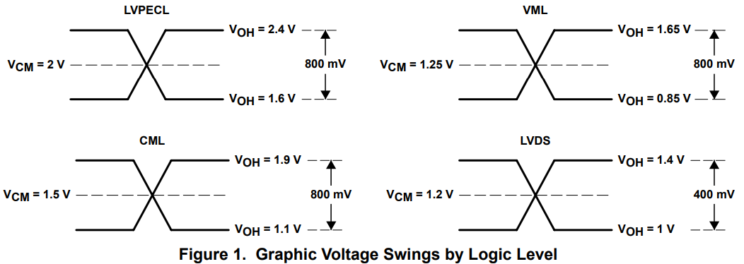
differential 신호의 로직 레벨을 볼때 알아야할 것이 common mode voltage와 swing voltage이다. differential 신호의 전압은 DC전압과 AC 전압으로 이루어져 있다. DC 전압이 common mode voltage, AC 전압이 swing voltage이다. 아래 그림 중 Graphic Voltage swings by logic level 부분에 표현되어 있다.
differential 신호 규격에 따라 DC 전압, AC 전압의 규격이 다르다. 아래 그림 중 voltage parameters by logic levle에 정리되어 있다.
- 전압 레벨에 따른 정리

- 회로 내부구조에 따른 정리
a. LVPECL - low voltage positive/pseudo emitter coupled logic
LVPECL is derived from ECL and PECL and typically uses 3.3 V and ground supply voltage.
>lvpecl은 ecl,pecl 규격에서 기원을 두고 있는 high speed 신호 규격이다.
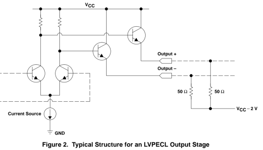
The typical output of an LVPECL driver consists of a differential pair with the emitters connected to ground via a current source. This differential pair drives a pair of emitter-followers which provide the current to Output+ and Output–.
>lvpecl의 출력은
접지에 붙은 전류원과 emitter에서 나오는 differential pair로 구성되어 있다. differential 출력은 두개의 differential 핀에서 전류를 출력한다.
The LVPECL output stage requires a termination resistance of 50 Ω to the bias voltage of VCC – 2 V.
> lvpecl의 출력부 회로에는 50옴 termination 저항과 Vcc - 2V 의 바이어스 전압이 필요하다.
This implies that the emitters of the pair of followers are around VCC – 1.3 V, because there is a 0.7-V drop across the base-emitter junction.
> 위에서 언급된 저항과 바이어스 전압으로 인해, Vcc가 3.3V라면 lvpecl의 common mode voltage가 2V 가 되도록 만들어준다.
The 0.7-V drop across the 50-Ω termination resistors results in a 14-mA flow through the PECL driver. Because the output impedance of the driver is lower than 50 Ω, care must be taken that correct termination is used to reduce voltage reflections that occur due to this mismatch.
>14mA 전류가 50옴에 흐를수 있도록 하는 로직이 LVPECL의 주요 특징이다. 그래서 termination 저항 50옴에 0.7V 전압이 걸린다.

The input stage consists of a differential pair which requires its inputs (Input+ and Input–) to be pulled up via resistors to VCC – 1.3 V in order to provide a common-mode voltage of 2 V in the case where VCC is 3.3 V.
> lvpecl의 입력으로 들어오는 신호의 common mode 전압은 2v가 되도록 외부에 termination 저항과 bias 전압을 걸어주어야한다.
b. VML
Texas Instruments voltage-mode logic (VML) drivers are voltage-level compatible with LVPECL. Like CML, these drivers are implemented in CMOS, but have the advantage that they do not require external pullup resistors, because of the use of internal NMOS and PMOS transistors to help drive the falling and rising edges. While VML is not yet as widely implemented as the other drivers, it still remains voltage-compatible with LVPECL signaling levels and has been used in many of TI’s production devices.
> VML은 LVPECl 규격과 같이 쓰기 편한 규격이다(??). VML규격은 PMOS, NMOS 트랜지스터 소자로 구성되어 있으며, 전류원이 아닌 전압원으로 구성한 회로이다. 따라서 출력으로 전류가 아니라 전압을 출력하기 때문에 LVPECL 또는 CML회로와 다르게, 전압신호를 출력하기 위해서 외부의 pullup(또는 termination) 저항이 필요가 없다는 특징을 가진다.

The PMOS and NMOS voltage-controlled voltage sources are used to set VOH and VOL of the driver, and the output transistor simply swings between those values. The output swing of VML interfaces is independent of the load impedance.
> VML 규격의 회로는 VoH 전압과 VoL 전압(위에서 언급된 전압레벨에 따른 분류 그림에서 언급된 용어)에서을 만들어주기 위해 전압원이 사용된 것이 특징이다. 전압원을 사용함으로써 VoH 전압과 VoL 전압 사이의 swing 전압을 쉽게 생성할 수 있다. VML 규격의 출력 전압은 출력에 연결되는 부하의 저항값에 독립적이다.(전류원이 아니라 전압원이기 때문에 가능한 것으로 보임.)
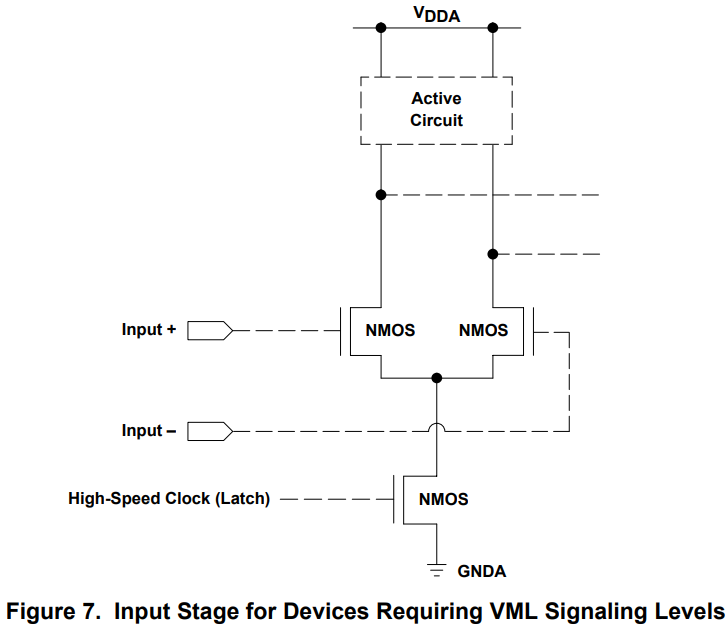
Similar to the CML receiver, the input stage for devices requiring VML signaling levels consists of a differential pair using NMOS transistors and the inputs (Input+ and Input–) need pullup resistors to the common-mode voltage of the receiver.
>vml의 입력부분 회로는 cml의 입력부분 회로와 비슷하다. vml에 입력( common mode 전압 + differential 전압)되는 전압은 2개의 nmos 트랜지스터에 연결되어 있다. common mode 전압을 만들어주기 위해서 pullup 저항을 vml 입력부에 달아주어야한다.
c. CML
The CML interface drivers provide several design features, including high-speed capabilities, adjustable logic output swing, level adjustment, and adjustable slew rate.
>cml 규격은 출력 swing voltage, slew rate를 조정할 수 있다는 특징을 가지고 있다.

The above devices have CML drivers that are built from an open-drain differential pair and a voltage-controlled current source using NMOS transistors.
>cml 규격 회로는 differential하게 구성된 open-drain회로와 전압제어형 전류원회로(nmos 트랜지스터로)로 구성되어 있다.
The outputs (Output+ and Output–) require pullup resistors to VDD because the NMOS transistor can drive only falling edges efficiently and needs the pullups to help drive rising edges.
>cml 규격의 출력회로 부분에는 vdd와 연결된 pullup 저항이 붙어있어야한다.
The voltage-controlled current source is used to vary the amount of current used to drive the load, because the output voltage swing is load dependent.
The load resistors and the external reference resistor can then be chosen to optimize output voltage swings
> cml규격의 회로는 전류원이 내부에 있는 것으로 볼 수 있다. 전류원의 전류를 조정하여 출력전압의 크기를 변동시킬 수 있다. 또는 출력부분의 swing 전압크기를 조절하기 위해 부하저항을 조절할수 있다.

The typical input stage for Texas Instruments devices designed for CML signaling consists of a differential pair using NMOS transistors, and the inputs (Input+ and Input–) require pullup resistors to the common-mode voltage of the receiver.
> vml의 입력부 회로부와 구조가 같다. cml 입력부 회로도 2개의 nmos 트랜지스터가 differential 신호와 연결되어 있으며, commonmode 전압을 만들어주기 위해 pull up 저항을 붙여야한다.
In the case of devices requiring CML voltage levels, the common-mode voltage should be in the range of 1.5 V. Where internal biasing is not included on-chip, this must be taken care of on the PCB, and the resistors should be placed as close to the device pins as possible.
> cml 규격에서 입력신호를 받아들일때 common mode 전압은 1.5v로 만들어주어야 한다.
The NMOS transistor attached to the drains of the differential pair acts as a latch and basically latches data in the receiver at the rate of the high-speed clock.
d. LVDS
The low-voltage differential signal (LVDS) standard is defined by ANSI TIA/EIA-644 and IEEE 1596.3–1996. LVDS has a lower swing and speed than LVPECL, CML, and VML, and therefore typically uses less power.
> lvds 규격은 lvpecl, cml, vml 보다
상대적으로 swing 전압이 작고, 지원하는 통신속도가 느리지만 상대적으로 적은 전력을 소모하는 장점이 있다.
Many LVDS drivers are built with constant current so power consumption does not scale with transmission frequency.
> 대부분의 lvds 규격의 회로들은 일정한 전류가 흐르도록 설계되어 있어서 전력소모량이 주파수에 따라 변하지 않는다. (?)

The LVDS output stage is similar to the VML driver except that Texas Instruments LVDS SERDES output structures use a feedback loop to regulate the common-mode output voltage of the driver.
This is shown is Figure 8. A current source attached to the drains of the NMOS transistors is used to control the output current, which is typically 3.5 mA, and provides a 350-mV swing across the typical 100-Ω termination resistor at the receiver.
> lvds 출력부 회로는 부하에 3.5mA 흐를수 있도록 하는 전류원이 포함된 것이 특징이다. 그래서 100 옴의 termination 저항이 lvds 입력부에 붙여져 있을때 양단에 350mV전압이 걸린다.
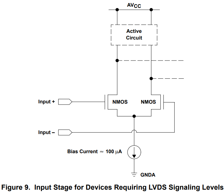
The typical input stage for TI’s LVDS-based SERDES devices consists of a differential pair using NMOS transistors, and the inputs (Input+ and Input–) require a 100-Ω termination resistor across the inputs with a common-mode voltage around 1.2 V.
> lvds 입력부 회로는 2개의 nmos 트랜지스터로 구성되어 있다. 또한 lvds 신호를 입력으로 받아들일때 100옴저항과 1.2v의 common mode 전압이 필요하다.
Where internal 100-Ω termination biasing is not included on-chip, this must be taken care of on the PCB, and the resistor should be placed as close to the device pins as possible. The current source attached to the drains of the NMOS transistors simply provides a small amount of current for the differential pair.
2. AC coupling과 DC coupling
회로 설계를 하다 보면 칩 A의 output 핀에서 나온 신호를 칩 B의 input 핀에 연결해야 하는 경우가 부지기수이며, 다반사이다. 특히 differential 신호 라인을 연결할 때 데이터 시트를 보면 AC coupling, DC coupling이라는 말을 자주 본다.
AC coupling, DC coupling이라는 단어를 접할 수 있는 곳이 바로 오실로스코프이다. 오실로스코프 프로브 설정을 하다 보면 AC coupling, DC coupling 설정을 하게 되어 있다.
DC coupling으로 설정 하면 프로브가 검출하는 신호의 DC 신호와 AC 신호를 전부 보여준다.
AC coupling으로 설정 하면 프로브가 검출하는 신호 중 DC 신호는 거르고 AC 신호를 화면에 보여준다.
이처럼 회로의 output 과 input을 연결할 때 언급되는 AC coupling, DC coupling의 개념은 오실로스코프에서 언급된 DC,AC coupling의 개념과 비슷하다.
다음그림은 lvpecl 규격의 출력신호를 다른 칩의 입력에 연결할때의 방법을 보여준다. ac coupling방법과 dc coupling 방법이 있다.
두 방법의 차이점 중 주목할 부분은 ac coupling의 경우 전송선에 커패시터를 달았다는 부분이다.
lvpecl 출력 신호
= common mode voltage(dc전압) + swing voltage(ac전압)
ac coupling을 이용한다면 커패시터에 의해
dc 전압은 다른칩의 입력에 전달되지 못하고 ac 전압만 다른칩의 입력에 전달될 수 있다.
예시는 lvpecl 출력을 lvpecl입력에 연결할 때이며
예시에서 커패시터를 제외하고 두 방법 중 차이가 나는 부분인 저항이나 bias 전압은 칩의 출력, 입력의 신호 규격(lvds, cml, vml)이 무엇인가에 따라 다르다.


3. termintation과 biasing
칩A의 출력을 칩B의 입력에 연결할 때 AC/DC coupling 말고 고려해야하는 점으로 termination과 biasing이 있다. 고속 신호 규격마다 common mode voltage와 swing voltage가 다르며, 신호 전송시 필요한 전류랑도 다르다. 따라서 칩의 출력과 입력 부분에 적절(?)하게 termination 저항을 달고 bias 전압 걸어주어야 한다. scaa059c, scaa062 문서를 보면 신호규격이 워낙 많기 때문에 수많은 termination 저항과 bias 전압 조합이 있다. 이 많은 조합을 scaa059c, scaa062 문서에서 잘 정리하고 있기에 필요하다면 이 문서를 보면 될 것 같다.
4. 예시
LVDS, LVPECL, CML 규격의 실제 사용예를 정리하였다.
Xilinx FPGA의 고속 트랜시버에서 사용되고 있었따. Xilinx사의 UG576 를 부분을 발췌하였다.
Xilinx FPGA 고속트랜시버는 클럭 입력을 받을 때 LVDS, LVPECL로 받을수 있었다.
-LVDS 예시

-LVPECL 예시

Xilinx FPGA 고속트랜시버 중 GTH모듈은 데이터 전송과 수신시 CML 규격을 이용한다.
- CML 예시
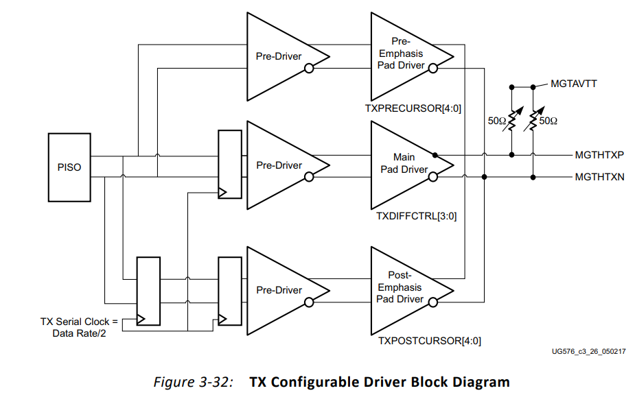

고속트랜시버의 데이터 송수신부의 신호규격은 LVDS가 아니라 왜 CML을 사용하는지 의문이 들었다. LVDS가 지원하는 데이터 속도는 < 2Gb/s 이하이며, CML은 >10Gb/s 이상이다. 고속트랜시버의 데이터 송수신 속도는 10Gb/s 이상이므로 데이터 송수신부는 CML로 설계되어 있고, 클럭 송수신부는 상대적으로 낮은 속도의 신호이면 되기에 LVDS로 설계된 것으로 보인다.
'고속통신신호 규격' 카테고리의 다른 글
| differential impedance란?? (0) | 2023.01.29 |
|---|---|
| 특성임피던스는 언제 필요하지? (0) | 2023.01.29 |